Welcome to an exhilarating dive into the realm of gaming nostalgia!
This tutorial promises to unravel the secrets of resurrecting the cherished GameBoy architecture on AMD's FPGA KR260. With a step-by-step guide, we aim to simplify this thrilling journey for you, ensuring that you can embark on this adventure with ease.
What's even better? We're generously sharing the open-source code on GitHub, inviting you to join the excitement and relive the enchantment of retro gaming firsthand!
The GameBoy Architecture
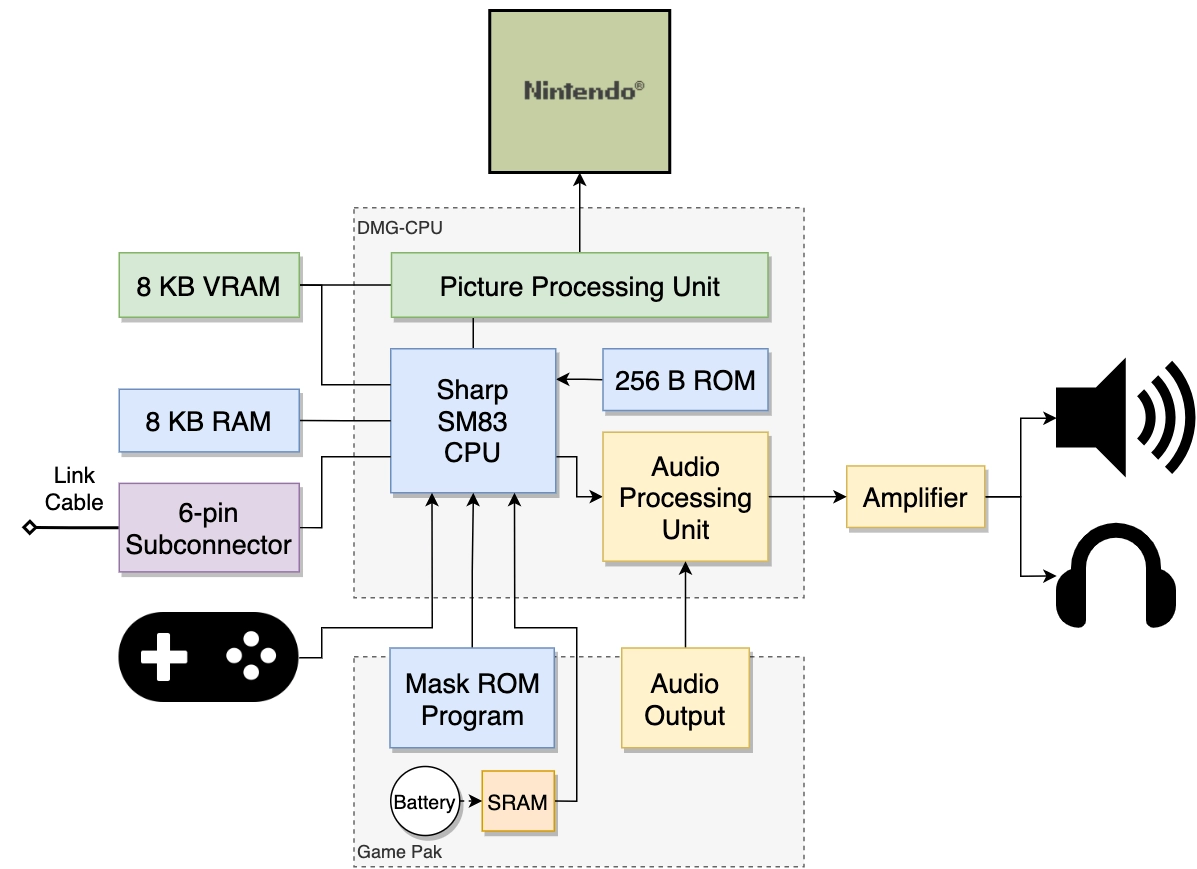
The GameBoy, a cherished handheld console, remains a marvel of simplicity and innovation. At its heart beats an 8-bit Sharp LR35902 processor, humming along at a modest 4.19 MHz. This processor not only executes game instructions but also deftly manages the system's memory and I/O operations.
Within the GameBoy resides an 8 KB internal RAM, serving as the repository for program data and in-game variables. Alongside this, there exists 8 KB of Video RAM (VRAM), meticulously allocated to render captivating graphics on the device's 160x144 pixel LCD screen.
Sound, an integral part of the GameBoy experience, is meticulously woven into its architecture. Boasting a 4-channel audio system, the console generates diverse waveforms and adeptly mixes them to produce an array of catchy tunes and immersive sound effects.
The backbone of the GameBoy's graphical prowess lies in its custom 8-bit GPU, functioning as the Picture Processing Unit (PPU). This dedicated unit supports a palette of 56 vibrant colors and is adept at displaying sprites and backgrounds through a variety of scrolling and tile mapping techniques.
Facilitating the use of game cartridges, the GameBoy incorporates a cartridge connector designed for external memory. These cartridges serve as vessels for additional ROM or RAM, enabling expanded game data and offering crucial save functionalities, enriching the gaming experience beyond the console's intrinsic capabilities.
The GameBoy Audio
The GameBoy's audio system is a charmingly straightforward yet remarkably versatile setup, comprising four distinct channels. Each channel serves a unique purpose, contributing to the immersive auditory tapestry that defines the gaming experience.
Square Wave Channel 1 (Tone 1 & Sweep): This channel is adept at generating square wave tones with adjustable frequencies and duty cycles. Its standout feature is the frequency sweep functionality, which creates a sliding effect, infusing the soundscape with dynamic variations and engaging nuances.
Square Wave Channel 2 (Tone 2): Much like its counterpart, this channel crafts square wave tones with independent frequency and duty cycle control. It enables the creation of harmonies and layered melodies, enriching the auditory landscape.
Waveform Channel (Wave): The Wave channel sets itself apart by utilizing a programmable waveform table. This feature allows for the playback of sampled sound effects or more intricate waveforms, offering a diverse range of tones and textures to enhance the audio experience.
Noise Channel: Adding an element of randomness and depth, the Noise channel generates noise-like sounds. Capable of mimicking percussion instruments, white noise, or various sound effects, it contributes significantly to the richness of the overall audio output.
These individual channels can be finely configured and artfully blended, affording game developers the opportunity to craft a rich and multifaceted soundscape within the constraints of the GameBoy's hardware. Through the seamless combination of these channels, developers were able to compose catchy tunes, atmospheric soundtracks, and memorable sound effects, contributing to the enduring allure of GameBoy games.
The VerilogBoy Project
VerilogBoy stands as an exceptional repository, offering a meticulously crafted and generic implementation of the iconic GameBoy architecture tailored explicitly for AMD's FPGA devices. This repository is a treasure trove, housing a comprehensive Verilog codebase that faithfully replicates the functionalities and behaviors of the original GameBoy hardware.
What sets VerilogBoy apart is its unwavering commitment to precision and detail, ensuring seamless compatibility and reliable performance specifically on AMD FPGAs. This precision makes it an invaluable resource not just for FPGA enthusiasts but also for retro gaming aficionados and developers keen on delving into the realm of GameBoy emulation on FPGA platforms.
Whether you're exploring the depths of FPGA technology, reliving the nostalgia of retro gaming, or seeking to delve into the intricacies of GameBoy emulation, VerilogBoy stands ready as an indispensable repository, offering a gateway to an authentic and immersive GameBoy experience on AMD's FPGA devices.
Fantastic! It sounds like you're ready to embark on an exciting journey of porting the VerilogBoy repository, which encompasses several crucial components for emulating the GameBoy architecture.
Here's a glimpse of what this repository comprises:1. CPU Implementation with Controller Input: This core component is the brain of the emulation, responsible for executing game instructions and handling input commands from the controller.
2. Bootable and Configurable ROM: A vital element, the ROM serves as the foundation for the GameBoy software, providing the initial boot sequence and configurable options for the emulation.
3. Cartridge Paging (MBC5): This component manages the cartridge's memory banking, particularly crucial for games utilizing Memory Bank Controllers (MBC5) to access additional memory beyond the GameBoy's native limitations.
4. PPU (Pixel Processing Unit): The PPU is the visual powerhouse, managing pixel rendering, sprites, backgrounds, and overall graphic processing.
5. Sound Unit: An integral part of the GameBoy experience, this unit handles audio generation, delivering the iconic tunes and effects that enhance gameplay immersion.
With these fundamental components in place, the process of porting begins! Each component requires meticulous attention and integration within the AMD FPGA environment. This endeavor promises an immersive and authentic GameBoy emulation experience tailored for AMD's FPGA devices. Are you excited to dive into this emulation journey, or is there anything specific you're curious about or need assistance with as you begin the porting process?
The GameBoy Implementation
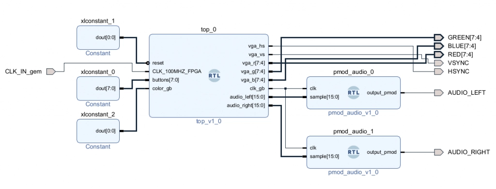
The Top module presents two implementation modalities: the block design flow and the Verilog Top Flow. Opting for the Verilog Top Flow appears preferable due to the complexity of the design and the multitude of different IPs involved. The full code repository is available for reference.
Let's delve into the Top module for analysis:
Inputs:
- reset: A wire signaling the system reset.
- CLK_100MHZ_FPGA: The 100 MHz clock input from the FPGA (for KR260, initially set to the carrier card oscillator at 25MHz, later configured through the Clocking Wizard).
- buttons: An 8-bit wire receiving input from the GameBoy buttons.
- color_gb: A wire indicating whether the GameBoy should output in color or grayscale.
Outputs:
- vga_hs, vga_vs: Wires for horizontal and vertical sync signals for VGA output.
- vga_r, vga_g, vga_b: 4-bit wires for red, green, and blue color components for VGA output.
- clk_gb: Output clock signal synchronizing GameBoy operations.
- audio_left, audio_right: 16-bit wires representing left and right audio channels for audio output.
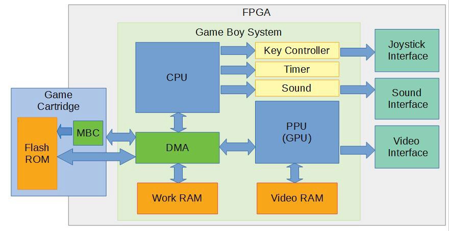
The code comprises instantiations of various modules such as PLL (Phase-Locked Loop), utilized as a Clocking Wizard IP for generating distinct clock signals. Additionally, it includes the Boy module responsible for GameBoy system emulation, the MBC5 module managing memory bank controller operations, and the VGA mixer module for generating VGA output signals.
Connections to other modules are also established. For instance, connections to the cartridge for reading ROM and RAM data, the single-port RAM for managing cartridge RAM operations, and the vga_mixer module for combining GameBoy image data with the VGA signal are included in the codebase.
This intricate configuration suggests a comprehensive emulation setup, interconnecting various components to emulate the GameBoy system accurately while ensuring synchronization, signal processing, and interfacing with external devices like the VGA output and audio channels.
The Audio Output Module
The "pmod_audio" module plays a crucial role in managing the audio output, functioning as a sigma-delta modulator employing a PWM (Pulse Width Modulation) DAC.
Here's a breakdown of its components and connections:
Inputs:
- clk: Input clock signal operating at a frequency of 21.477 MHz.
- sample: A 16-bit wire receiving audio sample inputs. The module operates with a sampling rate of 42 kHz.
Outputs:
- output_pmod: PWM signal output for the Pmod audio module.
Internal Signals:
- counter: A 9-bit register serving as a counter, controlling the timing for audio output.
- audio_latched: A 16-bit register used to store the latched audio sample.
- aud_pwm: A 1-bit register representing the PWM output signal.
The module operates within an "always" block triggered by the positive edge of the clk signal. Key operations occur within this block:
1. Latching Audio Sample: When the counter value is 0, the current sample value is latched into the audio_latched register.
2. PWM Generation: The aud_pwm register is set based on the counter and audio_latched values. If the counter is less than 1 or the concatenation of the counter with 7 zeros is less than audio_latched (within a 512 sample range), aud_pwm is set to 1; otherwise, it's set to 0.
3. Incrementing Counter: The counter value is incremented by 1.
4. Assigning Output: Finally, the aud_pwm register is assigned to the output_pmod wire, representing the PWM output of the module.
In summary, this module facilitates audio output by employing a PWM signal generated from the input audio samples, effectively utilizing the specified sampling rate to reproduce audio output.
Load New Cartridge
In the Vivado environment, a COE (Coefficient) file holds significance as a text-based format used for describing memory initialization files (MIF) within a digital design. Specifically, it serves to initialize memory blocks like ROM or RAM, outlining the initial values to be loaded into designated memory locations.
The COE file format embodies lines of data representing memory addresses and their corresponding values. Each line typically includes the memory address paired with its associated data value. Additionally, the file may contain supplementary details such as memory width, radix, or data organization, providing a structured format for memory initialization.
In the context of GameBoy cartridges within Vivado, the process involves converting the original cartridge dump file into a COE file compatible with Vivado's memory initialization requirements. This conversion process entails parsing the data from the cartridge dump and arranging it in the specific structure mandated by the COE file format.
Once the conversion is complete, the resulting COE file serves as an input for Vivado's memory initialization phase. Vivado utilizes this COE file to initialize the memory blocks within the FPGA design, effectively infusing the GameBoy emulator with the contents of the custom GameBoy games or applications extracted from the cartridge dump.
By leveraging the COE file's ability to initialize memory blocks in Vivado, users can expand the functionality of their GameBoy FPGA implementation. This allows for the loading and execution of a broader spectrum of GameBoy games and software, enhancing the emulator's capabilities and versatility.
Utility Tools
The "bin2hex_coe.py" script housed in the repository's "tools" folder serves a vital purpose: converting a cartridge dump file into both a hexadecimal file and a COE file, streamlining the integration of custom cartridges into FPGA designs.
Here's how the script operates:
1. Hexadecimal Conversion: It reads the binary cartridge dump file and translates its contents into a human-readable hexadecimal format.
2. COE Conversion: Simultaneously, the script generates a COE file from the binary data. This COE file adheres to the specific structure required, detailing memory addresses and their corresponding data values. By parsing the binary file, the script meticulously arranges the data to construct the COE file in the expected format.
Running the "bin2hex_coe.py" script on a cartridge dump file produces two essential outputs: the hexadecimal representation for human-readable data inspection and the COE file for seamless integration with tools like Vivado. While the hexadecimal file aids in understanding the contents of the cartridge dump, the COE file enables effortless utilization within FPGA designs or other tools that demand memory initialization files in COE format.
This script significantly simplifies the conversion process, empowering users to work effortlessly with custom cartridges. It grants accessibility to FPGA designs, allowing for the expansion and customization of the GameBoy FPGA implementation by effortlessly incorporating diverse cartridge dumps.
Load The COE File Into The Design
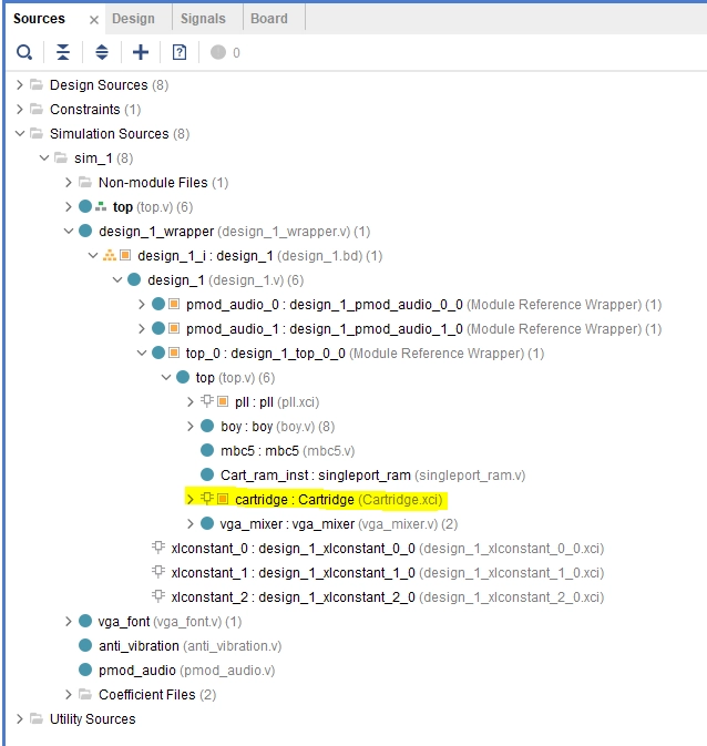
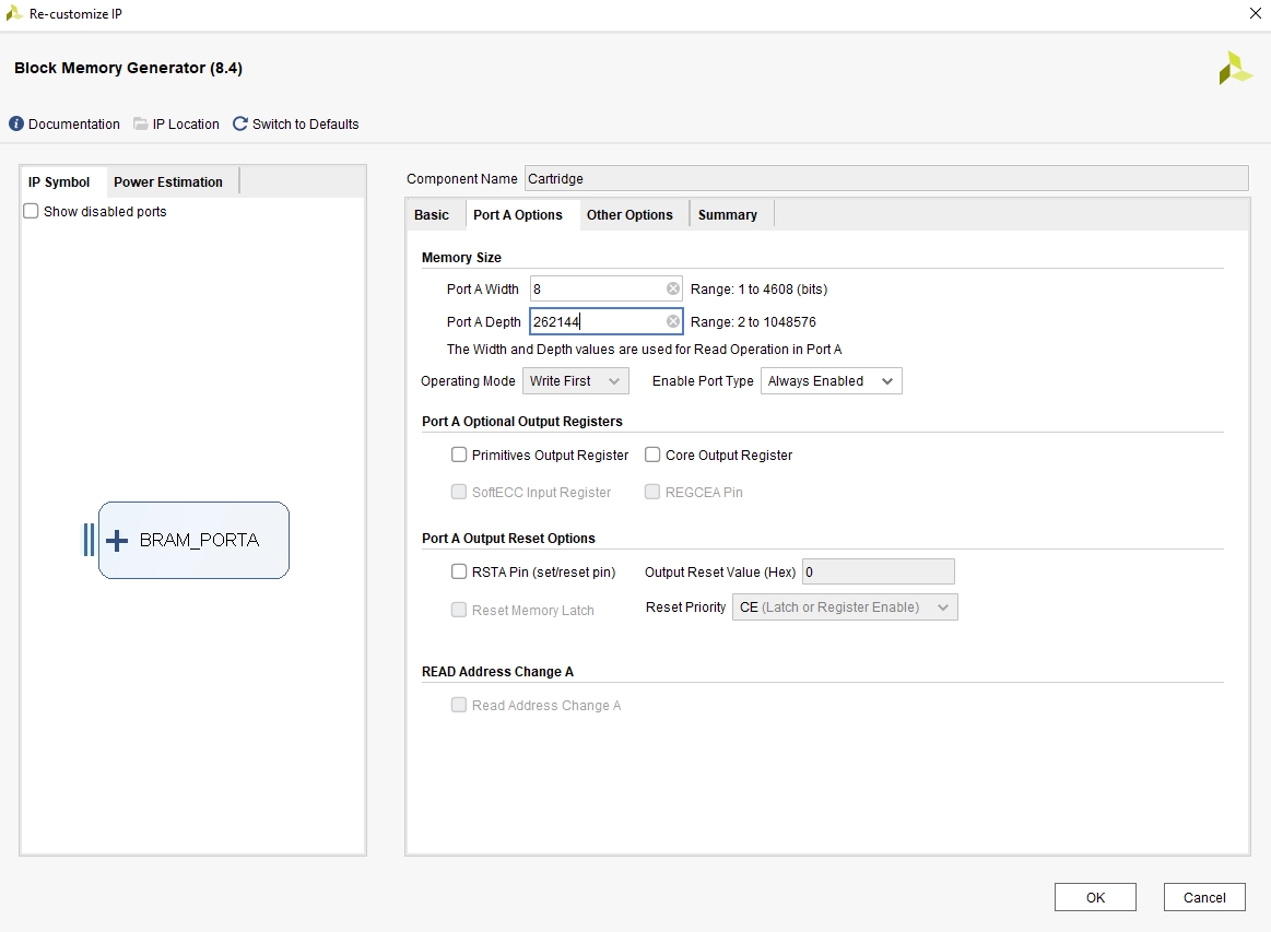
Certainly! Here are step-by-step instructions to load the COE file into the "Cartridge" IP core within the Vivado design:
1. Open Vivado Project & Access IP Inspector: Launch the Vivado project and locate the IP Inspector panel, usually situated on the left side of the interface.
2. Find "Cartridge" IP Core: Using the search or manual navigation within the IP Inspector, locate the "Cartridge" IP core among the listed IPs.
3. Re-customize Cartridge IP: Right-click on the "Cartridge" IP core and select the "Re-customize IP" option. This action will open a configuration dialog box specifically tailored to the Cartridge IP core.
4. Memory Initialization or Content Configuration: Within the configuration dialog, seek out the option related to memory initialization or content settings. This section allows you to specify the memory content source.
5. Specify COE File Path: In the memory initialization or content option, specify the precise path to the COE file that you intend to load into the Cartridge IP core. This path directs Vivado to the exact location of the COE file.
6. Save Configuration Changes: Once the COE file path is defined, save the configuration changes made within the dialog box.
7. Re-implement or Regenerate Design: To ensure the changes take effect, re-implement or regenerate the design in Vivado. This step applies the updated configuration settings to the Cartridge IP core, incorporating the specified COE file as the memory initialization data.
By following these steps, you'll successfully integrate the COE file into the "Cartridge" IP core, enabling the FPGA design to utilize the content from the loaded cartridge dump. This process ensures that the GameBoy emulator running on the FPGA can access and execute the game or application contained within the COE-loaded cartridge.
Port Depth Size Of The ROM
Absolutely, aligning the memory size in the Cartridge IP core with the content from the COE file is crucial for accurate emulation within the FPGA design. Here's how to adjust the memory size based on the number of lines in the COE file:
1. Specify COE File in Cartridge IP Configuration: As mentioned earlier, select the COE file path in the memory initialization or content option of the Cartridge IP core configuration dialog box.
2. Open COE File: Use a text editor to open the COE file.
3. Count Lines: Within the COE file, count the total number of lines. Each line in the COE file corresponds to a memory location and its associated data value.
4. Adjust Memory Size in Cartridge IP Core: Using the information gathered from the COE file, modify the memory size configuration in the Cartridge IP core. Match the memory size setting to the total number of lines counted in the COE file.
5. Save Configuration Changes: Once the memory size is adjusted to match the number of lines in the COE file, save the changes to the Cartridge IP core configuration dialog.
6. Re-implement or Regenerate Design: To apply the updated memory size configuration, re-implement or regenerate the design in Vivado. This ensures that the Cartridge IP core's memory capacity precisely accommodates the entire content from the COE file.
By meticulously adjusting the memory size in the Cartridge IP core to align with the content loaded from the COE file, you ensure that the ROM memory within the FPGA accurately mirrors the data from the GameBoy cartridge dump. This alignment is essential for seamless emulation and flawless execution of the GameBoy program on the FPGA design.